Optically switchable power electronic component (light-controlled cascode or super cascode)
// Electric Circuits // Electronics and Electrotechnology // Energy Transfer // Semiconductor
Ref-Nr: 16489
Abstract
The invention concerns an optically controllable, power electronic component or a corresponding circuit arrangement. This makes it easier and more reliable to design power electronic devices such as self-guided power converters, DC converters, inverters, switches for AC or AC loads and switches for DC loads.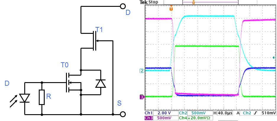
Figure 1: Circuit diagram of the light-controlled cascode (left), time sequences when switching on and off the test setup of the light-controlled cascode (right)
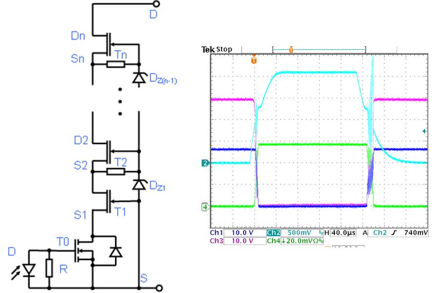
Figure 2: Circuit diagram of the light-controlled supercascode (left), time sequences when switching on and off the experimental setup of the light-controlled supercascode (right)
background
The optical control of a power semiconductor via optical fibers (FO), which ensures separation of the electrical potential, simplifies the design of a power electronic converter. Previously, there were only light-controlled thyristors that could be optically switched on but not off. This disadvantage is overcome by the inventive solution.
Motivation
Power electronic devices must have a galvanic potential separation of the control. This can be achieved by optical fibre using power semiconductors which can be switched on and off optically and which also have advantages in terms of electromagnetic compatibility.Innovation / Solution
With the invented solution, a controllable, power electronic component can be optically switched on and off. A photodiode supplies the gate voltage and charge for driving a normally-off semiconductor T0, such as a MOSFET. If the MOSFET is operated in a cascode or super cascode, T0 only needs to be designed for a low reverse voltage, the total reverse voltage of the (super) cascode is taken up by the other normally-on semiconductors T1 (up to Tn). Therefore, it is sufficient to generate the gate charge required to drive a low blocking semiconductor with a photodiode. It would be particularly advantageous to realize both the photodiode D and the normally-off semiconductor T0 as well as the resistor R on a common chip made of e.g. GaN. This chip, together with other normally-off semiconductors, could then be integrated into a common package to form an optically switchable power semiconductor with scalable blocking voltage. If the photodiode and the semiconductor T0 are composed of a wide-bandgap semiconductor such as GaN, a relatively high voltage of the photodiode results and at the same time a particularly low forward resistance RDSon of the semiconductor T0 can be achieved with the gate charge. Fig. 1 on the left shows the circuit arrangement of the light-controlled cascode according to the invention. When exposed to light, the photodiode D generates a voltage to drive the normally-off semiconductor T0, which in turn switches on the cascode. When the light signal ends, the resistor R discharges the gate circuit of T0, causing the cascode to switch off. Thus the light controlled cascode takes over the function of a MOS-FET or IGBT with the difference that it is an optical control e.g. via an optical fibre. Therefore the light-controlled cascode has only the two main connections Drain (D) and Source (S), an electrical control connection is omitted. Fig. 1 on the right shows the time course of a test setup of a light-controlled cascode. A load of 150 Ohm was switched at a voltage of 300V, the switched power is therefore 600W. Due to a lack of commercial availability, the GaN photodiode was replaced by an inverse blue LED and the normally-on semiconductor T1 was replaced by a 600V (normally-off) Si-MOSFET which received a positive gate bias voltage of 7V by a Z-diode and a capacitor, giving it normally-on behavior. Using a normally-on semiconductor for T1 would eliminate this bias. The individual curves show: Ch1 (blue): UDS of T0, 2V/division Ch2 (cyan): UGS of T0, 500mV/division (zero line other than Ch1 to 3) Ch3 (magenta): UDS of entire cascode, 50V/division Ch4 (green): ID of the cascode, 0.5A/division Time axis: 40µs/division The slow switching behaviour is due to the fact that an inverse LED was used instead of a GaN photodiode due to a lack of commercial availability. With an optimized photodiode made of GaN, its short-circuit current would be higher and the discharge resistance R could be smaller, which would accelerate both the charge and the discharge of the gate circuit. Fig. 2 left shows how the concept of the light controlled cascode can be extended to a super cascode. This allows the total reverse voltage to be increased and the component to be scalable in terms of its maximum reverse voltage. When additional stages are added, voltage symmetry is achieved by the Zener or suppressor diodes DZ1 to DZ(n-1) shown. Fig. 2 on the right shows the time course of a test setup of a two-stage light-controlled super cascode, i.e. the part of Fig. 2 on the left that is shown below the three points. A load of 340 Ohm was switched at a voltage of 500V, so the switched power is 0.735kW. Again, the inverse blue LED was used as photodiode and the normally-on semiconductors T1 and T2 were replaced by 600V (normally-off) Si-MOSFETs, which received a positive gate bias voltage of 9.5V by two 9V batteries each, giving them normally-on behavior. Using normally-on semiconductors for T1 and T2 would eliminate these batteries. The individual curves show: Ch1 (blue): Drain potential T1, 100V/division Ch2 (cyan): UGS of T0, 500mV/division (zero line other than Ch1 to 3) Ch3 (magenta): UDS the Super Cascode, 100V/Division Ch4 (green): ID of the cascode, 0.5A/division Time axis: 40µs/division You can see how the 250V suppressor diode limits the reverse voltage from T1 to approx. 250V. The reverse voltage of the super cascode exceeding this must be taken over by T2. This test setup also results in relatively slow switching for the reasons mentioned above. Also an oscillation during switching is recognizable which has to be damped by suitable circuits.Benefits
Optical switching on and off of a power electronic component
Wide range of applications due to scaling of the reverse voltage / especially in the range of higher reverse voltages
Independence of the control side of the (super) cascode from the entire reverse voltage
fields of application
Fields of application can be energy technology, electrical energy supply and transmission and drive technology.You can close this window. You can find your search results in the previous window