Sensor component and installation method – Transmission of thin-film structures
// Mechanical Engineering // Production Technology // Sensors and Measuring Instruments
Ref-Nr: 16490
Abstract
The technology relates to a transfer process of thin film microstructures produced on surfaces that can not be coated directly in PVD (cathode sputtering) systems due to their size or properties.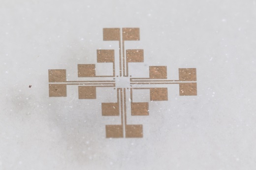
Coated PVD film substrate (example structure)
background
The use of PVD systems for coating components requires a vacuum environment. The vacuum systems limit the use of any size components, furthermore, a chemical reaction of certain materials during the sputtering process can not be excluded.Therefore, in this novel process, the component to be coated and the vacuum process are separated from each other.
Innovation / Solution
The innovation of this process is the use of a film-based coating technology with water-soluble polyvinyl foils to be coated and functionalized using PVD equipment. This can be done according to the state of the art in the roll to roll process. Subsequently, the coated film substrates are applied to the desired component, using chemical adhesives or surface functionalization. Subsequently, the water-soluble film substrate is removed to expose the conductor or sensor layer for contacting. In this method, the component to be coated does not have to be introduced into the vacuum chamber of the PVD systems and is therefore not limited in size or shape. A chemical reaction of the part during the PVD process can also be excluded. In addition, there is no temperature influence on the component, which can occur during PVD processes. An additional factor is the time savings in the production environment.Benefits
Coating of surfaces of large components. Use of flexible carrier substrates allows coating of complex surface geometries
No temperature influences on the target component, no unwanted chemical reactions during the PVD process
Flexible coating process
fields of application
PVD processes Production of z. B. sensor components microstructuringYou can close this window. You can find your search results in the previous window